

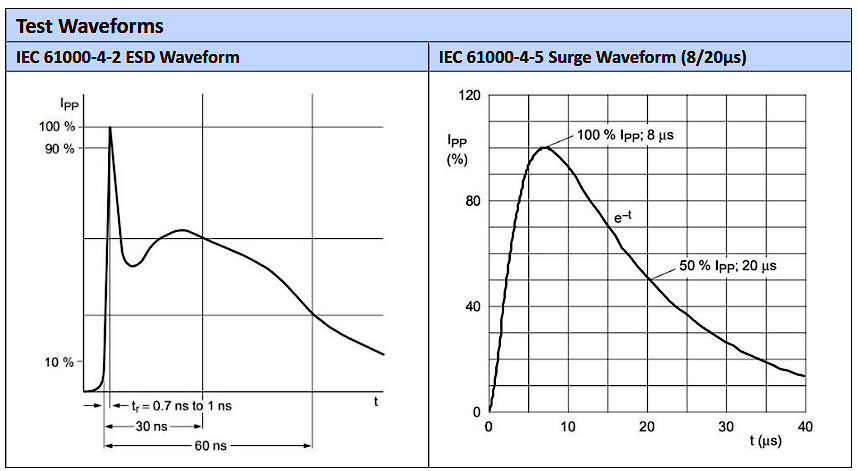

Some microcontroller pins interface almost directly with connectors or other device components exposed to external factors. In all such situations, effective protection against ESD and other overvoltages must be ensured. Importantly, such protection must be meticulously implemented and adapted to the type of signal.
Basic design assumptions
The VRWM voltage value of the TVS diode should cover the highest expected operating voltage occurring on a given line during normal operation, naturally taking into account power supply tolerances and the component tolerances as well. It is important to remember that VBR denotes the breakdown voltage at a specified test current, and VC denotes the clamping voltage at a given peak current. We described these and other parameters in the second part of this series. However, only the VC value, along with the overvoltage resulting from connection inductance, allows for estimating the actual maximum voltage present on the microcontroller line during an electrostatic discharge, as well as during EFT disturbances or surges. Crucially, we must compare parameters measured for the same pulse waveform. This means that datasheet values provided by the manufacturer for an 8/20 µs pulse cannot be directly treated as the peak voltage during an ESD discharge. For example, an SMBJ5.0A type TVS diode from Akyga Components has VRWM = 5.0 V, VBR = 6.4…7.0 V, and a maximum VC = 9.2 V at 65.3 A for a 10/1000 µs pulse—however, these data do not define the behavior of the TVS diode under ESD pulse conditions with a rise time four orders of magnitude faster.
Some datasheets also provide characteristics obtained using the TLP method, i.e., Transmission Line Pulsing. These allow for the evaluation of the clamping voltage as a function of current and the dynamic resistance of the protector and are useful when selecting ESD protection, although they do not replicate the entire discharge waveform according to IEC 61000-4-2 (specifically its initial peak). Interestingly, despite a completely different measurement methodology, the TLP technique refers to the test levels defined in the 61000-4-2 standard.

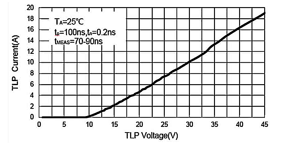
To evaluate the voltage at the protected input, it is also advisable to utilize response waveforms from actual ESD excitation and to consider the estimated inductance of the connections.
However, the mere presence of a transil (even a properly selected one) does not guarantee 100% protection for the microcontroller’s GPIO. Although a well-implemented TVS diode, placed near the connector or user interface element (e.g., a tact switch button), will absorb the main voltage surge, an additional series resistor may still be necessary. Its purpose is to limit the residual current, which will then be absorbed, for example, by the built-in GPIO protection diodes. The permissible injected current into I/O lines, including the total for the entire system, should be checked in the specific microcontroller’s documentation. However, it’s important to remember that this parameter does not declare the input’s immunity to short ESD pulses. What’s more: discharging current to the power rail also requires protecting the power supply circuit against voltage increase and considering the system’s behavior when a discharge occurs with the power supply off.
Analog inputs
A particular case that always requires careful analysis during embedded system design is the analog input. This can be either the input line of an ADC converter, a comparator, an internal operational amplifier, or another analog block working with a high impedance signal source . The TVS leakage current ( ), flowing through the equivalent resistance of the source (), introduces additional voltage error to the circuit. For a simple model, one can estimate its value as:
For calculations, we assume the maximum value (rather than the typical one). , and we also verify the voltage and temperature conditions of the specification.
For example: the previously mentioned ESD0501BU TVS diode has a maximum leakage current of 100 nA at a reverse voltage of 5 V and a temperature of 25°C. At this corresponds to a voltage error of approximately 1 mV. In the case of a typical 12-bit ADC operating at a 3.3 V reference voltage, 1 mV slightly exceeds 1 LSB, which will be acceptable in most applications. Of course, we are referring here only to the error component introduced by the TVS diode itself, whereas in reality, the overall ADC accuracy is also affected by dozens of other application factors.
Fast digital interfaces
Selecting TVS diodes for the protection of high-speed digital interfaces, such as USB or HDMI, is particularly demanding in terms of parasitic capacitance. If the capacitance is too high, it can significantly degrade signal integrity and increase the transmission error budget. The maximum allowable capacitance is determined by the rise/fall times required for a given interface type, rather than just the clock frequency itself.
In a simplified lumped circuit, the additional capacitance C, along with resistance R, would yield a 10-90% rise time of approximately . For a line with 50 Ω impedance and 100 pF capacitance, we would obtain a value of 11 ns, and for 0.4 pF, it would be just 44 ps. This is, of course, merely a comparison of scale, as in a real transmission line, the influence of capacitance also depends on the source and load impedance, or the point where the surge protector is connected. However, the given example clearly demonstrates the significance of additional capacitances introduced into transmission lines.
The ESD0501BU TVS diode, already mentioned several times in this article, offers a typical capacitance of 0.25 pF and a maximum of 0.4 pF at 0 V and a frequency of 1 MHz. An alternative for several data lines (e.g., within two USB 2.0 ports) is the SRV05-4 model, which offers a maximum capacitance of 0.7 pF between I/O and ground and 0.4 pF between two I/O lines. It should be noted that these values describe different measurements—in the case of the single-channel ESD0501BU transil, specifying inter-channel capacitance would, for obvious reasons, make no sense.
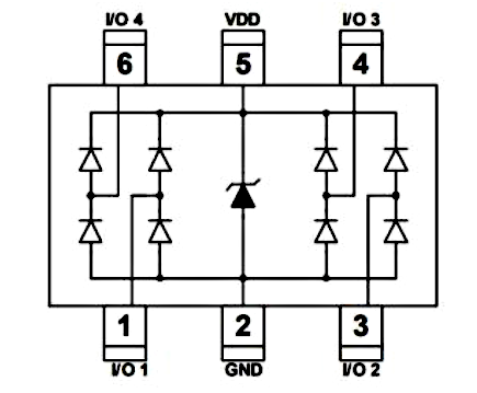
Importantly, low capacitance alone does not determine protection effectiveness: the ESD0501BU model has a maximum VC = 25 V at 4 A @ 8/20 µs, while the SRV05-4 has nearly half that, only 13 V under the same measurement conditions. On the other hand, the first of the mentioned models has a declared ESD immunity level 5 kV higher in the contact discharge test (20 kV vs. 15 kV for the SRV05-4) and nearly twice the declared pulse power for an 8/20 µs waveform (100 W vs. 55 W).
For digital interfaces, however, leakage current is of somewhat less importance than parasitic capacitance. In most typical embedded systems, additional nanoamperes drawn from transmission lines should not visibly degrade signal integrity.
Regular I/O ports
For buttons, alarm inputs, or various control signals, a higher capacitance may be acceptable (and in some cases even welcome—the TVS diode’s capacitance, on the order of hundreds of picofarads when connected in parallel to a given line, works with the resulting series resistance to form an additional RFI filter). Leakage current can also be ignored in many cases, provided, of course, that it does not interfere with the circuit’s operation. Two factors must be taken into account here.
First, it is important to remember to check the leakage current when designing a battery-operated device. This issue is particularly prevalent in common TVS diodes with relatively high peak power (hundreds of watts) and VR in the range of a few volts. Leakage current in the order of several hundred microamperes can far exceed the power budget of the entire device in sleep mode.
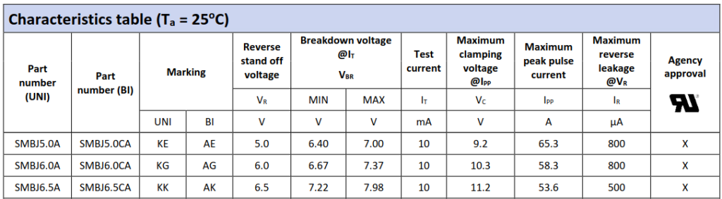
Secondly, a larger leakage current must be taken into account in those parts of the circuit that contain pull-up resistors with a resistance of several kilohms or more. In an extreme case, the leakage can be large enough to cause a microcontroller’s digital input to misinterpret the signal. Let’s assume that an SMBJ series TVS diode with a VR voltage of 5 V is connected in the circuit of a tactile switch, which is pulled up to the positive power rail using an external 4.7 kΩ resistor. With a current of 800 µA, a voltage drop of up to 3.8 V can occur across this resistor. In a 5 V supply voltage system, this will result in a off-state voltage of approximately 1.2 V at the microcontroller’s input, which falls within the range of 0 V to 0.3VCC (0…1.5 V), interpreted—for example—by a 5-volt ATmega microcontroller as a logical low state. From the MCU’s perspective, the TVS diode will therefore simulate a short circuit of the input to ground via the switch, making it potentially… impossible to distinguish its actual state!
Summary
Ensuring the required level of protection for microcontroller inputs or outputs against high-voltage disturbances is not a trivial task. While selecting a TVS diode begins with determining the operating voltages and permissible peak voltages, it concludes with verifying a series of specific requirements for a given part of the circuit. In an analog path, one of the primary parameters will often be the leakage current of the TVS diode, whereas in the case of digital interfaces, it will be the parasitic capacitance, which affects signal integrity. Even for simple binary inputs/outputs or power supply circuits, an improperly selected TVS diode can significantly degrade parameters or even prevent the normal operation of the device.
As if that were not enough, the ultimate effectiveness of microcontroller protection is drastically influenced by the proper implementation of the protection device within the PCB design. We will address this aspect in the fourth and final part of this series.
Sources
- Akyga ESD0501BU, 2023-09, rev. 1
- Akyga SMBJ5.0A(CA)-SMBJ440A(CA), 2023-09, rev. 1
- Akyga SRV05-4, 2025-09, rev. 1
This article is sponsored by Akyga Components
Akyga Components offers a wide range of electronic components for industrial and consumer electronics. The brand’s portfolio includes primary and rechargeable batteries, semiconductors, passive components, power supply and circuit protection solutions, which are used in automation, IoT, lighting, and measurement systems. For more information visit www.akygacomponents.com